Tel.: 0532-89226888
English
Products & Services
PRODUCT
Conductive silicon carbide substrate
Foundry Services for Slicing, Grinding and Polishing
Wafer Thinning
Reclaim wafers
Detection Services
conductive silicon carbide substrate

Products

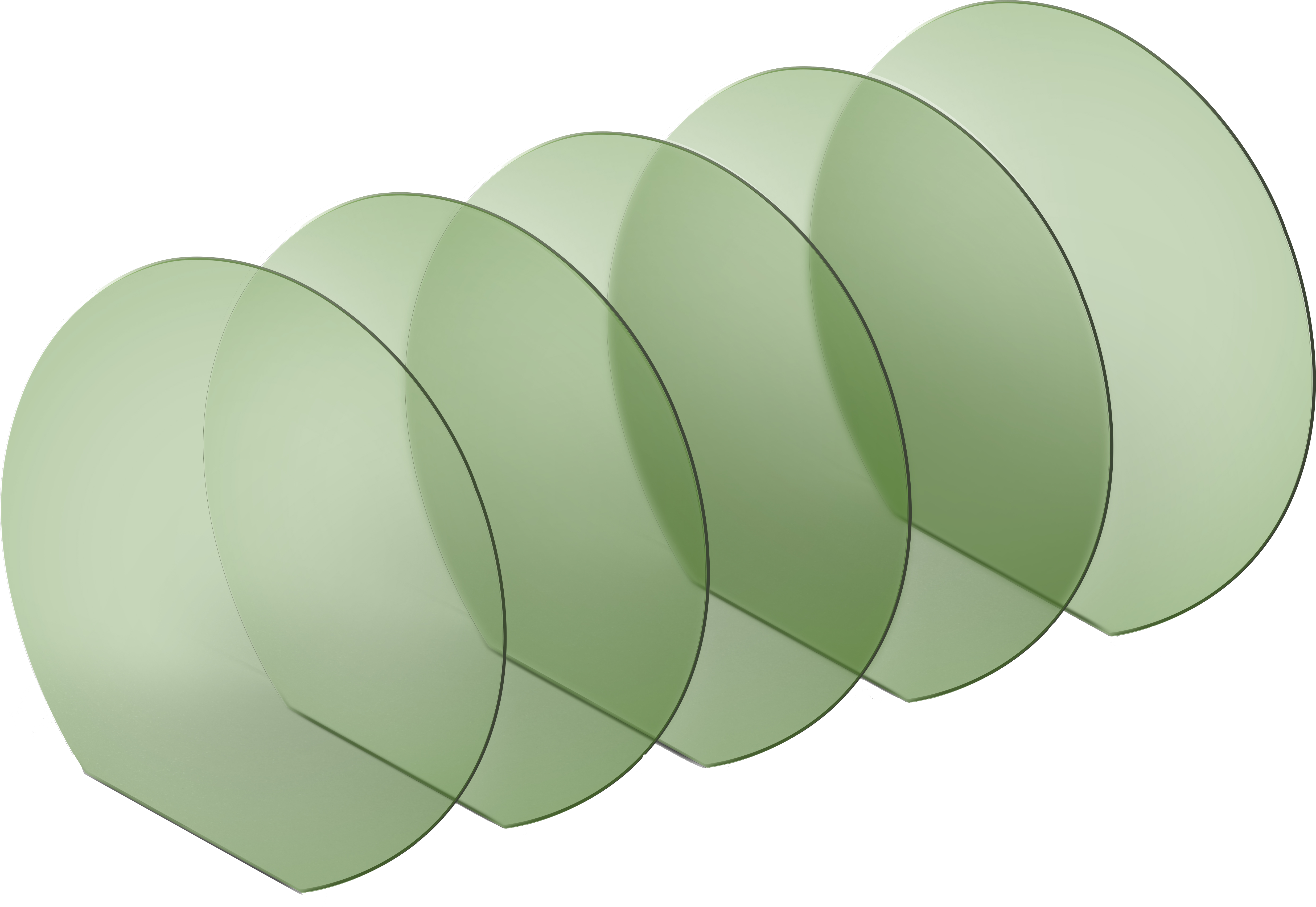
Substrates are the underlayer materials of all semiconductor chips, playing the role of physical support, heat conduction, conductivity, etc. According to the latest survey by TrendForce, due to the rising popularity rate of electric vehicles and the trend of 800V high-voltage electric vehicle architecture, the global automotive market demand for 6-inch conductive silicon carbide substrates is expected to reach 1.69 million pieces in 2025. Because of the complex manufacturing process of SiC substrates, high technology access threshold, and slow growth, the upstream supply of SiC substrate materials will become the major bottleneck in the production of SiC power devices. Most n-type SiC substrates for power semiconductor devices are 6 inches in diameter.


Future Prospect
Six-inch conductive silicon carbide substrate will remain the mainstream until 2027. Thanks to the explosive growth of the electric vehicle market, the penetration of SiC power devices in automotive applications far exceeds market expectations. The obtaining ability and cost of silicon carbide substrate will in turn directly determine the deployment speed of 800V charging architecture in electric vehicles.
Application Scenarios
The main role of silicon carbide in semiconductors is to act as a substrate material. Silicon carbide substrate is the cornerstone of the application of gallium nitride and silicon carbide in third-generation semiconductor materials. Silicon carbide materials are used in various power devices mainly because of the epitaxial growth of silicon carbide epitaxy layers on conductive silicon carbide substrates. In recent years, due to the maturity of the technology process and the decline of the preparation cost, the application in the field of new energy continues to expand. The reason silicon carbide has become an important basic material for the development of the third-generation semiconductor industry lies in its superior physical properties: high band gap (corresponding to a high breakdown field and high power density), high electrical conductivity, and high thermal conductivity. Therefore, it is expected to become a widely used basic material for making semiconducting chips in the future.
Foundry Services for Slicing, Grinding and Polishing
01
Step 1 Slicing:
use wire to slice ingots into wafers.
02
Step 2 Grinding/polishing:
remove the damaged layer caused by the previous workstation, and make the flatness and roughness of the wafer meet customer requirements.
03
Step 3 Cleaning/Inspection:
It is to remove the residual abrasive and metal during processing, and use relevant instruments to inspect the flatness, particles, defects, etc. for customers to trace the quality of the wafers.
Wafer Thinning

Product Introduction
Silicon carbide wafer thinning technology meets the high market demand for thin, light, short, high-performance and energy-saving semiconductor elements. It is widely used in HEMT、MOSFET、Schottky Diode, etc.


Main functions
Reduce on-resistance

Improved thermal efficiency


Products and services
Wafer thinning of 6-inch and 8-inch

Reclaim wafers

Product Introduction
A considerable number of dummy wafers will be used by wafer fabs and epitaxial fabs in the manufacturing process, the first test wafer after equipment maintenance as well as defective wafers produced in the process. After metal removal (if there are circuits already), grinding, fine polishing, CMP and cleaning, these wafers will go through a series of inspection procedures equivalent to those for standard wafers, so as to ensure that the quality meets the customers’ needs for reuse.

We can provide services for reversed polishing of wafers for wafer fabs and epitaxy fabs. Since the silicon carbide substrate accounts for 50% of the production cost of power devices, both wafer fabs and epitaxy fabs need to recycle qualified substrates for reasonable use.


Products and services
Reclaim wafers of 6-inch and 8-inch

Detection Services
Professional inspecting equipment and professional services
ICP-MS/MS 8900
(Inductively coupled plasma mass spectrometer): Metal ion detection.
Tropel
(Flatness measurement equipment):Substrate morphology detection, TTV, Bow, Warp., etc.
Napson
(Resistance meter): Substrate resistance measurement.
CANDELA 8520
(Defect detector): substrate defect detection, scratch, particles, pit, micropipe, etc.
TOP