Comparison of physical properties
Restricted by its performance, the first-generation semiconductor is not suitable for use in fields such as high temperature, high voltage, high frequency and high power.
Compound semiconductor normally refers to crystalline inorganic compound semiconductor, that is, a compound formed by two or more elements in a determined atomic ratio, with the characteristics of high electron mobility, high band gap, etc., which can be used in high temperature, high voltage, high frequency and other environments.
Compound semiconductor normally refers to crystalline inorganic compound semiconductor, that is, a compound formed by two or more elements in a determined atomic ratio, with the characteristics of high electron mobility, high band gap, etc., which can be used in high temperature, high voltage, high frequency and other environments.
Si
First generation
GaAs
Second generation
GaN
Third generation
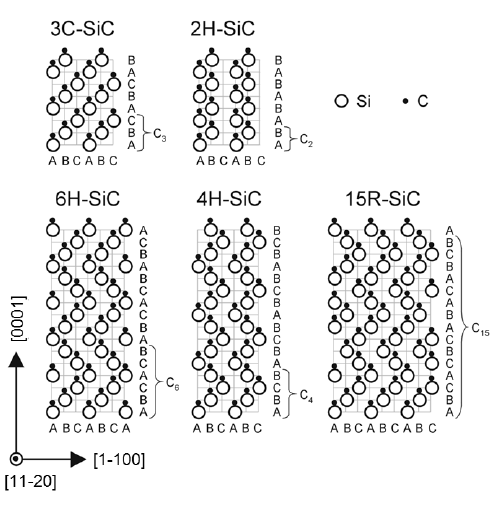
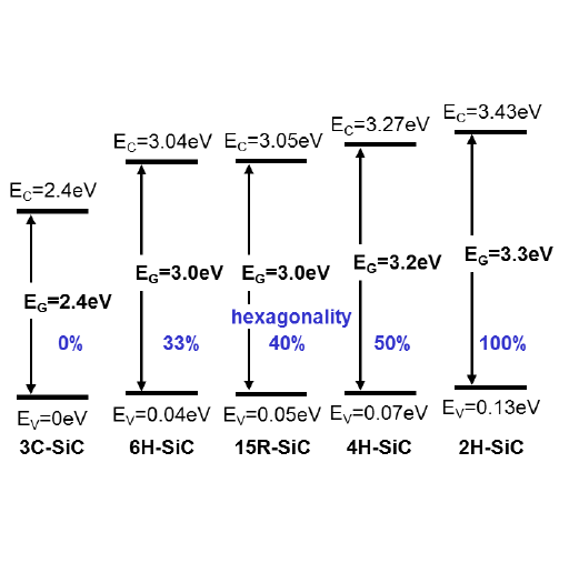
4H-SiC
4H-SiC
6H-SiC
6H-SiC
3C-SiC
3C-SiC
Third generation—SiC